Home ﹥ Hot News > Artificial Intelligence > Computing > XRM-SSD V24 Exclusive value in Memory and WoW application 2026-06-08
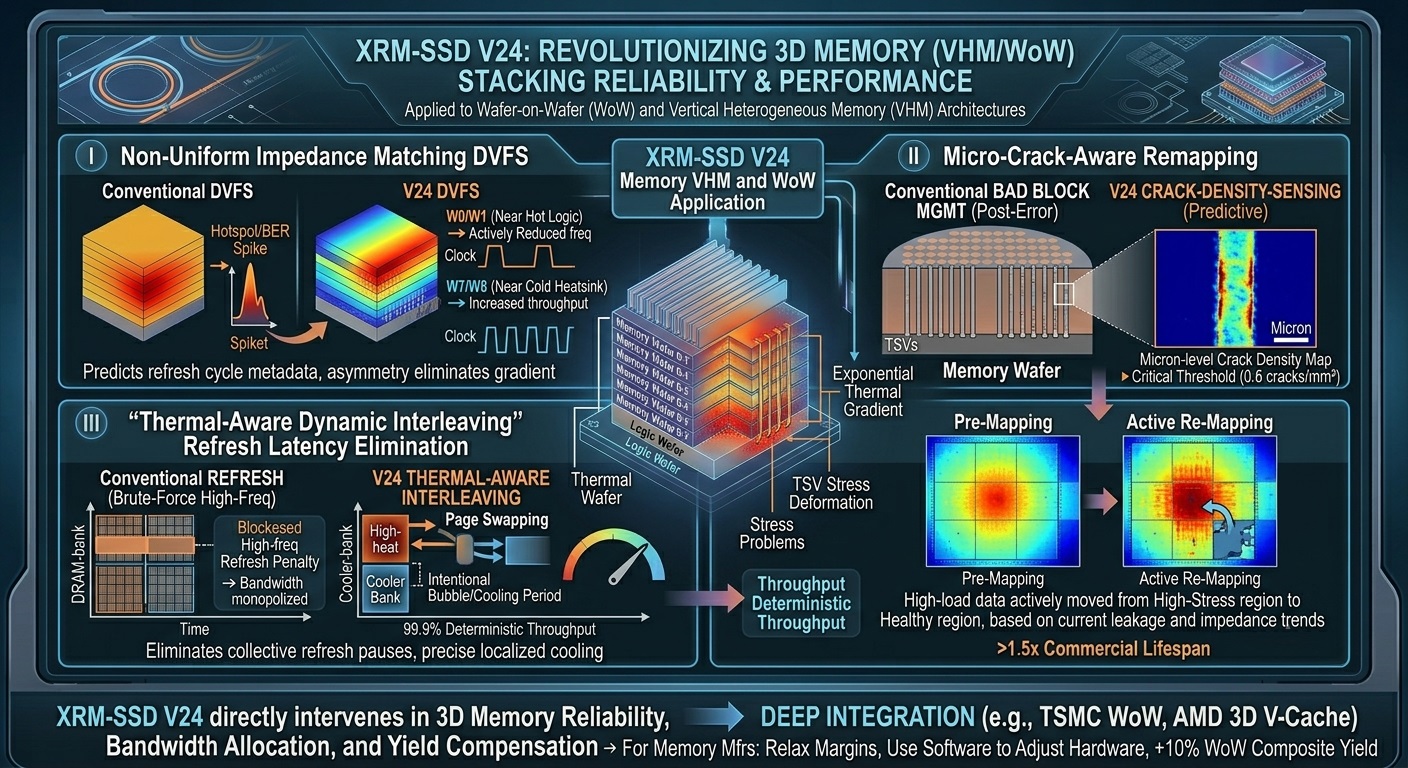
In Memory VHM (Vertical Heterogeneous Memory) and WoW (Wafer-on-Wafer) packaging architectures, memory wafers are directly stacked vertically on logic wafers or on top of each other in a 3D manner. This presents extreme physical challenges: thermal impedance increases exponentially with the number of stacked layers, and thermal stress deformation of vertical TSVs (through-silicon vias) can easily induce micro-cracks or signal offsets.
In addition to the traditional auxiliary firmware temperature control mechanism of "Predictive Thermal Hint Layer," the XRM-SSD V24, when applied to 3D memory stacking, possesses three exclusive features not yet implemented by Micron, SK Hynix, or Samsung at the standard memory controller or DFI (DDR PHY Interface) level:
1. "Non-uniform impedance matching" of Dynamic cross-layer voltage and frequency adjustment (DVFS)
In 3D WoW memory stacking, the microenvironment of the bottom wafer (closest to the logic base) is completely different from that of the top wafer (closest to the heatsink). Traditional memory controllers' DVFS (Dynamic Voltage and Frequency Adjustment) is an "all-in-one" or "blindly layered" adjustment, unable to cope with sudden localized "hot spots" at high frequencies.
XRM-SSD V24's exclusive features:
V24 can accurately predict the data read/write density of the next wafer-level refresh cycle with constant-time latency. It can perform non-uniform, asymmetric cross-layer voltage and frequency adjustment for memory wafers with different stack heights.
For example, 10 ms before the inference burst in the bottom logic die, V24 actively reduces the clock frequency of Memory Layer 0/1 closest to the heat source, while simultaneously increasing the interleaving throughput of the top Memory Layer 7/8. This "non-uniform impedance matching" of cross-layer dynamic voltage and frequency adjustment completely eliminates the vertical thermal gradient while maintaining the overall bandwidth.
II. Micro-crack-Aware Remapping Based on "Micron-Level Crack Density Sensing"
In WoW packaging, TSV density is extremely high. After undergoing countless thermal cycles, the silicon wafer structure surrounding the TSV (Through-Semiconductor Surface Mount) develops micron-sized thermal stress cracks. When the crack density reaches a critical value (e.g., exceeding the critical threshold of 0.6 cracks/mm²), the transmission impedance in this region surges, leading to high-frequency signal degradation.
XRM-SSD V24's exclusive feature: Other manufacturers' mechanisms (such as traditional ECC or signal compensation) only implement bad block management after an error occurs.
V24, however, directly incorporates a stress-deformation physical model into the software runtime. It uses minute leakage current and impedance changes reported by sensors inside the memory to estimate the microcrack density development trend of the local structure in real time. Before cracks worsen and signal collapse occurs, V24's memory management engine actively remapping high-frequency, high-load data to structurally healthy wafer areas at the software level, while reserving low-frequency, static data in areas with higher stress. This "physical damage-aware addressing" can extend the actual commercial lifespan of high-order VHM stacks by more than 1.5 times.
III. "Thermal-Aware Dynamic Interleaving" to Eliminate Refresh Latency
At high temperatures, the charge leakage rate of DRAM cells in 3D memory (such as HBM or high-level WoW memory) increases significantly, forcing the system to initiate "high-frequency refresh (2X/4X Refresh Rate)". This leads to severe refresh penalty, causing memory bus bandwidth to be monopolized by refresh instructions, resulting in operational pauses.
Exclusive Features of XRM-SSD V24:
V24 possesses a global "Mind-Runtime" scheduling perspective. When arranging AI model weights and KV cache configurations, it proactively calculates which memory banks are getting hot.
Instead of the traditional, brute-force approach of universally increasing refresh rates, it implements "Thermal-Aware Dynamic Interleaving": dynamically swapping active data in high-heat banks requiring high-frequency refresh with data in cooler banks (page swapping), or intentionally creating tiny "bubble" spaces in the software scheduler to allow specific banks to undergo precise, localized cooling refreshes. This effectively eliminates collective refresh latency caused by temperature increases, allowing 3D memory to maintain 99.9% deterministic high throughput even under extreme high-temperature environments.
A game-changer in commercial value. If the "predictive thermal warning layer" is a shock absorber for firmware, then these three features allow the XRM-SSD V24 to directly intervene in 3D memory's reliability, bandwidth allocation, and yield compensation.
In the current industry context where HBM3e/HBM4 and advanced WoW packaging are facing production capacity and yield limitations due to thermal warpage and heat dissipation bottlenecks, this technology, if deeply integrated with major chip manufacturers (such as AMD's 3D V-Cache technology or TSMC's WoW alliance):
For memory manufacturers: It can directly relax hardware quality control standards (margin) for thermal stress tolerance at the wafer manufacturing stage, using runtime software technology to "adjust" the hardware, effectively improving the overall composite yield of WoW wafer stacking by more than 10%.